How to choose your routing class in AFNOR SPEC 2212
Video hosted by YouTube: playing it here means accepting YouTube's cookies.
As defined in the official AFNOR SPEC 2212 document, Routing Classes (RC), or Classes de Routage in the original French, are design rules enabling the routing of printed circuit boards. As we saw earlier, this concept is adapted from the former NF C93-713 standard.
There are 10 routing classes presented in AFNOR SPEC 2212, numbered RC1 to RC10. The higher the routing class number, the denser the printed circuit board can be.
RC10 is therefore the routing class with the highest density. It is important to note that, for the time being, this class is provided for prospective purposes. It will therefore be imperative to have this class validated by your printed circuit board manufacturer ahead of your project.
Organic substrates for semiconductors or SIP (System In Package) that require clearances/track widths beyond class 10 are not considered in this document.
Why classify printed circuit boards by density?
Densifying a printed circuit board is not without consequences. Reducing track sizes, reducing clearances, using buried vias, microvias and so on: all these changes make it harder for manufacturers to produce the printed circuit board. This leads to more scrap, the use of more expensive machines, more manufacturing steps, increased inspection and a host of other constraints.
Thanks to this classification, designers are now able to assess how complex their printed circuit board will be to manufacture, which gives them the opportunity to reduce costs and risks by choosing the lowest possible routing class and by adjusting the routing parameters whenever possible.

Why increase the routing class?
Your choice of components:
The first parameter that forces you to increase the routing class is often set by the package of the most constraining component on your board. The pin-to-pin pitch is a value you cannot change without forcing a change of component part number. Whether it is for drawing the land pads of your footprint or for breaking the tracks out of your component, the finer your component's pitch (the center-to-center distance between its two closest pins), the higher the routing class.
Your choice of board technology:
The choice of stackup (the structure and stacking of the layers) directly influences the density of your printed circuit board.
- Impedance-matched signals, which are directly tied to the stackup, may have track widths or clearances that impose a higher density and therefore a high routing class.
- The choice of vias also affects the density, but it also has a direct impact on how difficult the board is to manufacture.
Space on your printed circuit board:
If space runs out on your printed circuit board and the routing is stuck, increasing the routing class can be a solution. Thinner tracks, smaller vias and tighter clearances make routing easier in very dense areas.
How do you choose the routing class?
To choose your printed circuit board's routing class effectively, start by identifying the most constraining elements that cannot be modified.
It is therefore often wise to start selecting your routing class based on your components.
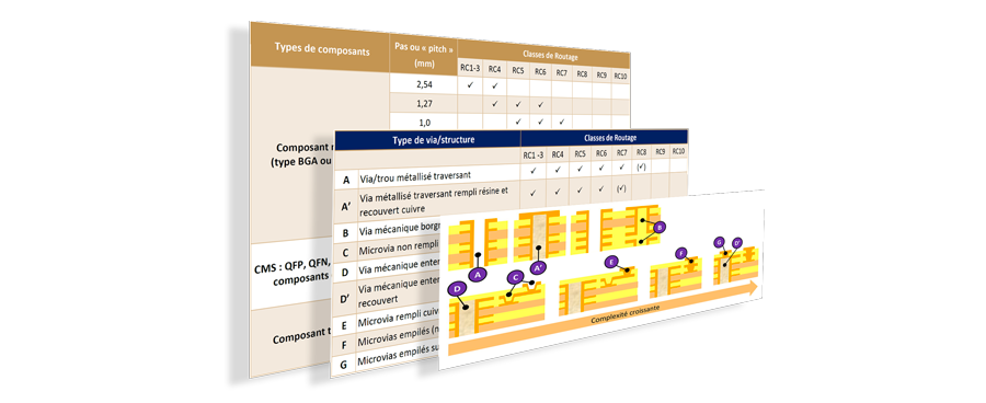
To that end, AFNOR SPEC 2212 provides a table in which components are categorized by type, then by their “pitch” (the center-to-center distance between pins).
In the table below, locate the component types and “pitches” present in your project. Then locate the associated “V” marks, which indicate the compatible routing classes to apply to your printed circuit board.
For example, for a BGA with a 0.8 mm pitch, the table tells us to use class RC6 or RC7.
Watch out for component compatibility!
Did you know that a BGA with a 1.0 mm pitch is not compatible (not recommended) with a BGA with a 0.4 mm pitch? Many factors come into play, whether at the level of PCB etching tolerances or related to solder paste deposition (different stencil thickness per area).
Have you identified incompatible components? Several solutions are available to you:
- Change components to an equivalent part number but with a different pitch.
- Plan ahead and contact your printed circuit board manufacturer and/or your EMS for the assembly of your boards in order to validate feasibility. Be aware that this solution will limit the number of manufacturers / EMS able to build your board and will take you outside the AFNOR SPEC 2212 classification.
Once the routing class has been identified, keep it in mind and look at the table below.
This table lets you choose the routing class according to the via/structure type that makes up your printed circuit board.
In this table, locate the via/structure types present in your project, then identify the associated routing class. If several via/structure types are present on your printed circuit board, it is important to select the most constraining type, and therefore the highest routing class.
For example, if a microvia not filled with copper is present, prefer routing class RC6. If your printed circuit board also includes stacked microvias, you will no longer be able to use class RC6. You will need to use at least routing class RC7.
Cells marked in parentheses (V) indicate via structures that are possible but that carry significant constraints on the conductor parameters on external layers.
Once you have obtained the routing class from both tables, compare these two values and select the more constraining one.
As with the component-type table, you will need to check compatibility within the table but also between the two tables.
Other constraints can increase your printed circuit board's class, such as the space available for routing, which we covered earlier. Since no table can list these constraints, you will need to draw on your experience or run an analysis to anticipate and determine the routing class associated with these other constraints. Fortunately, a tool is available on this site to make this choice easier. I will tell you about it at the end of this chapter.
Adapt and improve the result:
Analyze the constraints that led you to select your routing class, then locate these constraints on your printed circuit board. If these constraints are not present over the entire board, it is possible and preferable to lower the routing class in the areas that allow it.
This will reduce the manufacturing complexity of your printed circuit board.
In some routing software, it is possible to create constraint areas that differ from those applied to the rest of the board. Use this option as much as possible to increase the manufacturability of your printed circuit board.
It is essential to note that using a value belonging to a higher routing class than the rest of the board, even locally, will classify the entire printed circuit board in that class.
Make your choice easier and safer.
As we have just seen, choosing the class is essential to secure the fabrication of your PCB and to anticipate problems. However, the number of parameters to take into account can be daunting and lead you to choose the wrong class. That is why I invite you to use the “Choose your routing class” tool, which will let you select your class easily. Alerts are set up to flag incompatibilities, and dynamic drawings will let you anticipate the number of tracks you will be able to route between your vias, pins, etc., and thus better anticipate your needs.
FRANCE CAO encourages you to download and read the latest version of AFNOR SPEC 2212 on the official AFNOR website, to ensure a complete and accurate understanding of the document. FRANCE CAO declines any liability regarding the accuracy or completeness of the information provided, and strongly recommends consulting the official source directly for any specific use or interpretation.
FRANCE CAO has obtained the reproduction, publication and exploitation rights for AFNOR SPEC 2212, allowing it to use this data in accordance with the terms of the intellectual property rights concession agreement established with AFNOR.
© AFNOR Editions - AFNOR SPEC 2212, 2023. Tous droits réservés.
PCB design rules: which values should you choose?
What is AFNOR SPEC 2212?
How to choose your routing class in AFNOR SPEC 2212
Advanced use of the AFNOR SPEC 2212 dynamic routing class ta…
Interview - Christian Maudet - AFNOR SPEC 2212
Interview - Noémie Thoores - AFNOR SPEC 2212
AFNOR SPEC 2212 goes international: IEC PAS 63720